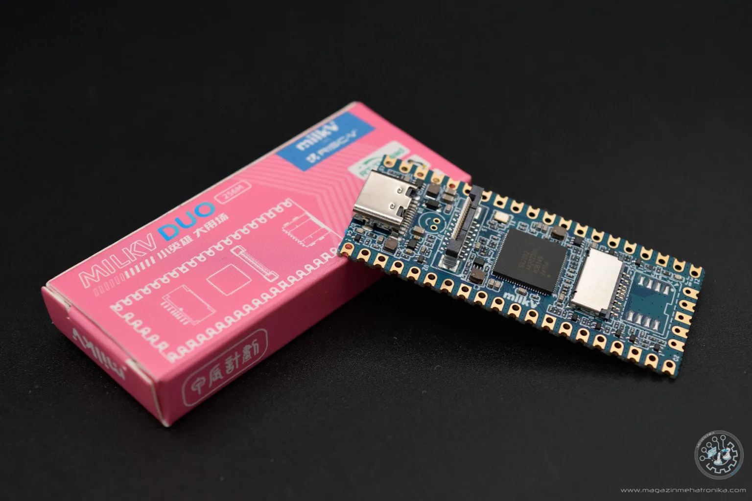
On a black tabletop, a blue circuit board leans against a pink box. It is scarcely longer than a stick of gum. A USB-C socket occupies one end; a camera connector, microSD slot, two ragged lines of solder pads, and the SG2002 system-on-chip fill almost everything else. This is the Milk-V Duo 256M, and it makes a better portrait of SOPHGO than a photograph of another conference stage.[2][3][10]
The usual account of China's AI hardware race begins in the datacenter: scarce accelerators, giant training clusters, domestic replacements for imported GPUs. SOPHGO belongs in that account, but its smallest products reveal a different contest. At the edge, a chip is useful only when a model can be converted, quantized, fitted into limited memory, joined to a camera pipeline, booted reliably, and maintained after the demo. Peak arithmetic is one line in that story. The compiler and board-support layers determine whether anyone can finish it.
As of 2026-07-19T07:37:28Z UTC, SOPHGO describes itself as a RISC-V-and-TPU computing company with products across cloud, edge, and endpoint. Its own timeline runs from the SOPHON brand in 2016, through SOPHGO's establishment in 2019, the CV180 edge family and BM1684X in 2022, BM1688 in 2023, BM1690 in 2024, and SG2044 in 2025.[1] The Duo does not summarize that whole catalogue. It exposes the company's operating thesis in miniature: processor architecture, neural accelerator, media hardware, compiler, SDK, and open-source enablement have to arrive together.
A product ladder, not one maker board
Milk-V's current documentation now labels the original Duo end-of-life and recommends the Duo 256M or Duo S. That change turns what looked like a novelty board into a compact product ladder. The original CV1800B Duo paired two T-Head C906 RISC-V cores with 64 MB of integrated memory and a 0.5 TOPS INT8 TPU. The same 21 × 51 mm outline now holds the SG2002 in the Duo 256M: 256 MB of memory, a 1 TOPS INT8 TPU, and a choice between a 1 GHz RISC-V C906 or a 1 GHz Arm Cortex-A53 as the main application core. The larger Duo S moves to 512 MB and adds onboard Ethernet plus optional wireless connectivity, while retaining the mixed RISC-V, Arm, 8051, and TPU design.[2]
Those are modest numbers by datacenter standards. That is the point. An edge camera or doorbell does not need to imitate a frontier chatbot. It needs to ingest a sensor stream, run a bounded vision model, encode video, respond within a power budget, and keep working without a permanent cloud connection.
The SG2002 packaging makes that use case unusually explicit. Milk-V's official material places the chip in IP cameras, smart peepholes, video doorbells, and home devices. Alongside the neural unit, the SoC includes H.264/H.265 video functions, an image-signal processor, a small 8051 subsystem, and security features intended to carry the system from development into a product.[3] Independent coverage in February 2024 confirmed the same physical proposition: a 256 MB board with camera input, microSD storage, USB-C, exposed I/O, and an accelerator, then selling for less than ten dollars before shipping.[9]
That low-cost board is not proof of commercial adoption. It is a distribution surface. A developer outside a large customer account can hold the architecture, inspect the public materials, and discover where the rough edges are. For a lesser-known Chinese chip vendor, that visibility has strategic value.
The compiler is the connective tissue
SOPHGO's most revealing public artifact may therefore be TPU-MLIR, not a chip specification. The open repository accepts models from common front ends including PyTorch, ONNX, TFLite, and Caffe. It exposes calibration and several precision paths, supplies model runners and validation tools, and lowers a model through an MLIR-based pipeline toward a device-specific executable.[4]
The underlying paper explains why this is more than a file converter. TPU-MLIR defines a hardware-independent TOP dialect for graph semantics and a hardware-aware TPU dialect for the target. A model is imported into the first representation, optimized, then lowered according to a chip's configuration. The authors also describe verification between transformation stages, because a successful compile is not useful if quantization or lowering silently changes the answer.[5]
That separation is the heart of SOPHGO's stack claim. Framework fashions can change above the compiler; memory layout, supported operators, local SRAM, precision, and scheduling remain painfully specific below it. A durable toolchain needs to absorb both kinds of change without asking application teams to rewrite a model for every processor generation.
The edge branch also makes clear that one family name does not erase deployment differences. Current TPU-MLIR examples for larger BM-class devices produce bmodel artifacts, while the CV18xx guidance lowers INT8 or BF16 models into a cvimodel for that edge line.[4][6] In both cases the workflow includes transformation, calibration or quantization, deployment, and comparison against reference outputs. The shared compiler structure matters; so do the distinct runtime contracts at the end.
This is where the Duo's severe memory limits become analytically useful. On a 256 MB system, “supports ONNX” is not enough. Operators must be covered, intermediate tensors must fit, preprocessing cannot consume the whole machine, and the chosen precision must preserve acceptable accuracy. The board turns abstract portability into a sequence of failures a developer can actually observe.
The camera stack is the product test
Compilation is only the middle of the journey. SOPHGO's TDL SDK sits closer to the application and shows what the company expects these processors to do. Its documentation describes a modular inference framework with image processing, memory management, model loading, preprocessing, tensors, video decoding, C/C++ and Python interfaces, and sample applications for face detection, landmarks, object detection, pose, tracking, licence-plate recognition, intrusion detection, and people counting.[7]
That list should not be read as evidence that every model is production-ready. It is evidence of where integration work accumulates. A smart-camera system must connect sensor capture to image processing, model execution, tracking, encoding, and application logic. If the SDK supplies only a fast kernel, the customer still has to assemble the rest. If it supplies a coherent pipeline but locks every component to one stale image, the apparent convenience becomes maintenance debt.
The Duo 256M review photographed for this article found exactly that tension. The reviewer could reach the board over USB networking and work with documented C examples, but described a constrained official image, host-side cross-compilation, separate software paths for RISC-V, Arm, and Arduino use, and interfaces that could not all be active together.[10] Those observations are not a verdict on a 2026 software release; they are a valuable 2024 baseline. They show how far the experience had to travel from “open documentation exists” to “an ordinary developer can own the full lifecycle.”
Open is a gradient
SOPHGO and Milk-V have made unusually substantial source material public for inexpensive silicon: datasheets, board files, SDK trees, compiler code, examples, and community channels.[2][3][4] The operating-system layer is less complete, and that distinction matters.
Upstream U-Boot documentation for the original Duo records a minimal but real boot path. It recognizes the CV1800B and builds a board target, yet the documented flow still relies on a vendor first-stage bootloader to initialize clocks and load U-Boot. The enabled mainline support described there is essentially the serial console; the sample boot log reports no Ethernet.[8] In other words, “supported upstream” and “all board peripherals work from upstream software” are very different claims.
This is not unusual for young embedded hardware. Camera interfaces, media engines, pin control, clocks, networking, and accelerators often reach a vendor SDK before they reach a general-purpose kernel. But the gap defines the ownership cost. A short-lived device can tolerate a frozen board-support package. A camera, gateway, or industrial sensor expected to receive security updates for years needs a cleaner answer about boot firmware, kernel versions, drivers, reproducible builds, and update recovery.
The dossier therefore has three clocks. Silicon advances when SOPHGO releases a new CV or SG part. Compiler support advances when models, operators, precisions, and target back ends become usable. Upstream support advances when the board can shed private patches and old vendor components. A launch looks complete only if those clocks are collapsed into one announcement. A deployment team experiences them separately.
Why the small board matters
The Duo family is not strategically important because a one-TOPS device will train large models. It matters because it makes China's edge-AI supply chain inspectable at developer scale. The board connects a Shenzhen hardware company, a Beijing-based processor vendor, T-Head CPU cores, a Chinese TPU toolchain, Linux and RTOS work, camera hardware, and global open-source projects in one object that costs less than many cables.[1][2][3]
It also shows why “domestic chip substitution” is too narrow a frame. SOPHGO is not merely trying to replace one foreign accelerator with a pin-compatible Chinese part. Its edge strategy mixes RISC-V and Arm application choices, a separate microcontroller, video blocks, and a proprietary neural unit beneath an open compiler. The switching cost sits across all of those layers. A cheap board lowers the cost of trying them; only stable software lowers the cost of keeping them.
Three developments would demonstrate that this strategy is maturing. First, new edge processors should arrive with model conversion, operator coverage, quantization recipes, and validation tools at launch rather than months later. Second, camera, networking, boot, and accelerator support should move steadily toward maintained upstream components. Third, independent users should be able to publish reproducible latency, power, accuracy, and memory results for complete pipelines—not just quote the TOPS line from a product page.
The falsifier is equally concrete. If the compiler grows for flagship parts while low-cost boards remain tied to fragmented images, partial peripheral support, and undocumented version combinations, the Duo will remain an engaging maker curiosity rather than proof of a durable edge platform.
For now, the board earns attention precisely because it refuses the glamour of the datacenter. It asks the harder, smaller questions. Can the model be lowered? Does it still agree with the reference after quantization? Will the camera feed arrive? Does the process fit in memory? Can the device boot from software someone can maintain? SOPHGO's edge-AI position will be decided by those answers, one 21 × 51 mm board at a time.
Sources
- SOPHGO, “About SOPHGO” (official company profile and development timeline for the SOPHON, BM, CV, and SG product families).
- Milk-V, “Milk-V Duo” documentation overview (current family status, processor, memory, TPU, interface, and operating-system specifications).
- Milk-V, “Duo 256M” getting-started page (official SG2002 architecture, intended edge-camera applications, media functions, TPU, compiler, SDK, and security framing).
- SOPHGO,
sophgo/tpu-mlir(official open-source compiler repository; front ends, lowering workflow, quantization, validation tools, current quick starts, and target artifacts). - Pengchao Hu et al., “TPU-MLIR: A Compiler For TPU Using MLIR,” arXiv:2210.15016v2 (2023; TOP/TPU dialect design, lowering pipeline, and transform-stage verification).
- SOPHGO, “CV18xx Guidance,” TPU-MLIR documentation (edge-family INT8/BF16 lowering and
cvimodeldeployment workflow). - SOPHGO, “TDL SDK Introduction” (official CV180x/CV181x application framework, modules, language bindings, and computer-vision sample catalogue).
- The U-Boot Project, “Milk-V Duo” board documentation for v2024.04 (upstream build path, vendor first-stage bootloader dependency, enabled driver boundary, and sample boot log).
- Jean-Luc Aufranc, “Duo 256M is a compact SBC based on SG2002 multi-architecture SoC,” CNX Software (February 13, 2024; independent launch-era hardware and software-resource inventory).
- Aleksandar Dakić, “Milk-V Duo 256M recenzija,” magazin Mehatronika (November 3, 2024; updated February 28, 2025; hands-on software observations and source of the documentary board photograph).